P-N junction diode
P-N junction is an interface or a boundary between two semiconductor material types, namely the p-type and the n-type, inside a semiconductor.
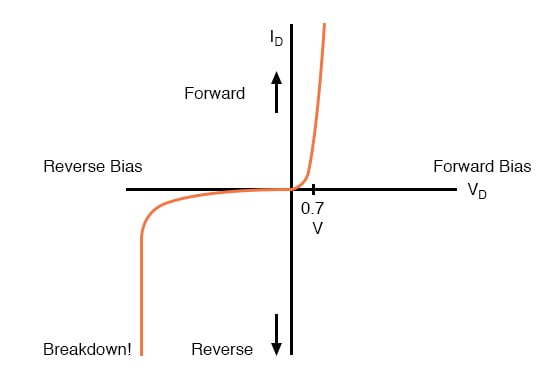
- The method of applying voltages to p-n junction diode is called biasing.
- There are mainly two types of biasing :
a) Forward biasing : The positive terminal of the voltage potential is connected to the p-type while the negative terminal is connected to the n-type.
b) Reverse biasing : The negative terminal of the voltage potential is connected to the p-type and the positive is connected to the n- type.
Forward biasing
When the P-N junction is forward biased, the built-in electric field at the P-N junction and the applied electric field are in opposite directions. When both the electric fields add up, the resultant electric field has a magnitude lesser than the built-in electric field. This results in a less resistive and thinner depletion region. The depletion region’s resistance becomes negligible when the applied voltage is large. In silicon, at the voltage of 0.6 V, the resistance of the depletion region becomes completely negligible, and the current flows across it unimpeded.

Reverse biasing
When the p-type is connected to the battery’s negative terminal and the n-type is connected to the positive side, the P-N junction is reverse biased. In this case, the built-in electric field and the applied electric field are in the same direction. When the two fields are added, the resultant electric field is in the same direction as the built-in electric field, creating a more resistive, thicker depletion region. The depletion region becomes more resistive and thicker if the applied voltage becomes larger.
Graph :
V-I Characteristics of P-N Junction Diode